
Quantum Matter for Optoelectronics

Topological materials are emerging as powerful platforms for next-generation optoelectronic technologies. Their unique electronic structures—characterized by topologically protected states—enable enhanced light-matter interactions, especially in chiral systems. In particular, chiral topological materials exhibit remarkably strong photogalvanic effects, making them highly promising for applications in quantum photonics and photovoltaics.
A key aspect of this behavior lies in the nonlinear electromagnetic response, which is directly governed by the quantum geometry of the electronic wavefunction. These effects are especially pronounced in systems with flat bands or band crossings near the Fermi level, such as topological semimetals, where discontinuities in the Berry curvature give rise to large, quantized responses. Not only do these nonlinear responses offer a route to technological innovation, but they also serve as sensitive probes of broken symmetries and quantum states that are otherwise difficult to detect.
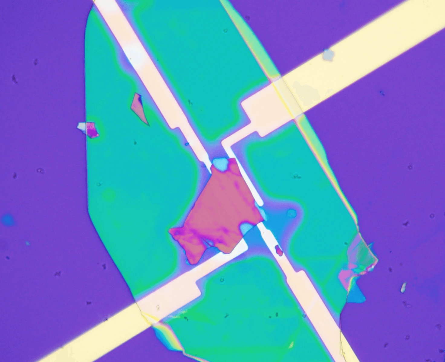
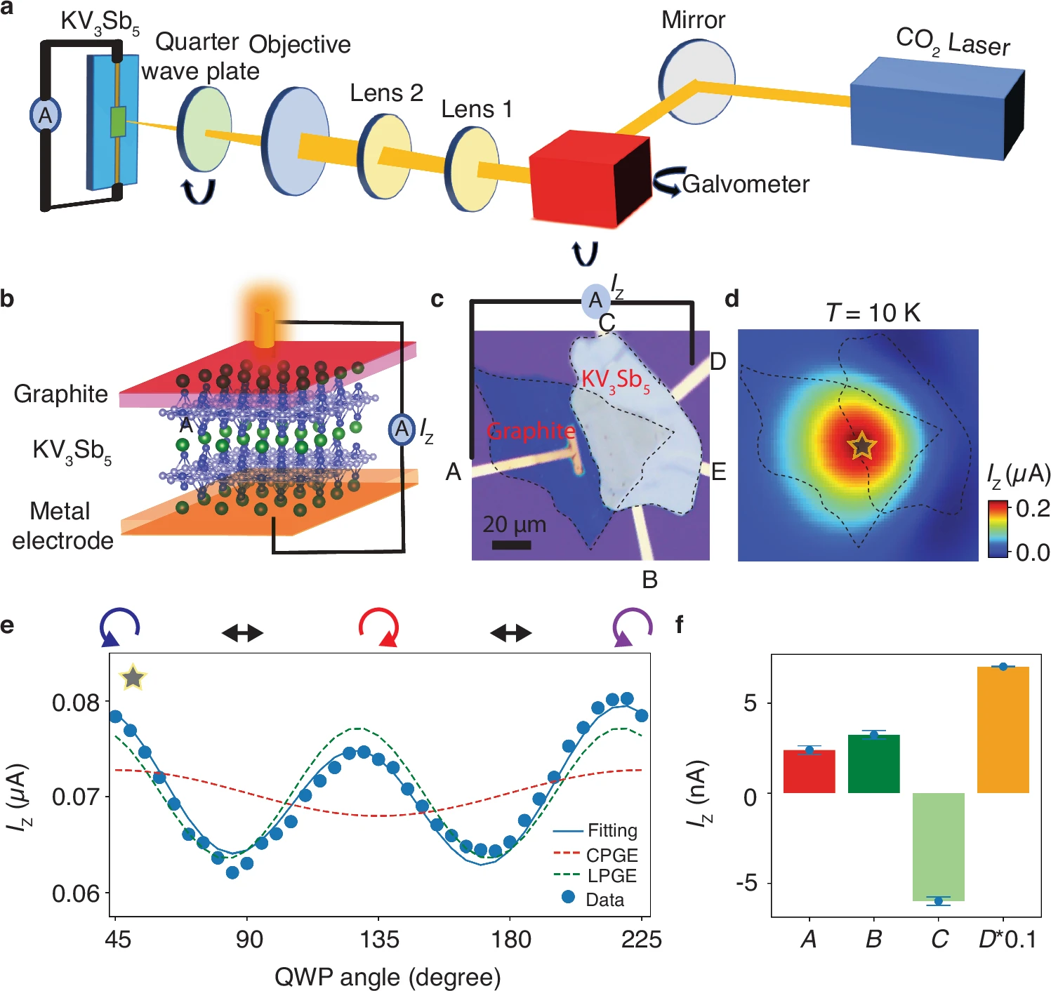
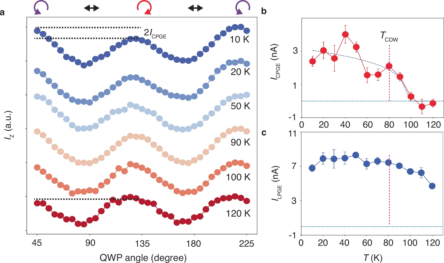
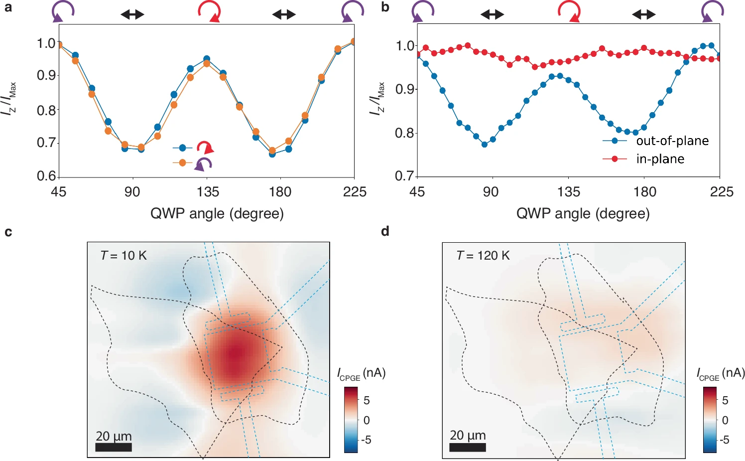
In our past research, we harnessed these principles to resolve a long-standing question in the topological kagome metal KV₃Sb₅—a material at the center of debate over whether it spontaneously forms chiral quantum states during its charge density wave transition. Conventional techniques struggled to detect the subtle symmetry breaking associated with these transitions, as the difference between left- and right-handed quantum states is exceptionally delicate.
To address this challenge, we developed a scanning photocurrent microscope capable of measuring nonlinear photocurrent responses under circularly polarized light—essentially, a quantum analog of the James Webb Space Telescope for materials. By fabricating ultra-clean KV₃Sb₅ devices and cooling them to cryogenic temperatures (~4 K), we revealed a striking phenomenon: at high temperatures, the material showed no preference for light polarization, but below the transition temperature, it developed a handedness in its photocurrent response—a clear signature of circular photogalvanic effect, and thus, of broken mirror and inversion symmetries.
This discovery does more than resolve a scientific controversy—it unlocks a new method for studying hidden quantum order and opens avenues for engineering chiral quantum states with practical applications. The ability of emergent chiral states to produce such pronounced nonlinear effects suggests exciting potential for next-generation optoelectronic and photovoltaic devices. Our work also demonstrates that second-order electromagnetic measurements are powerful, often underutilized tools for probing elusive symmetry-breaking phenomena in quantum materials.
Looking Ahead
Photocurrent Tunneling Microscopy: Visualizing Quantum Excited States at the Atomic Scale
We are developing a new frontier in quantum imaging by integrating scanning tunneling microscopy (STM) with scanning photocurrent microscopy to create a novel technique: photocurrent tunneling microscopy. This powerful hybrid tool will allow us to use light to excite and directly probe quantum states with atomic-scale resolution.
By mapping photocurrent generation with nanoscale precision, this method enables unprecedented access to the spatial distribution of photoexcited electrons and holes—providing a real-space view of excitonic processes at the atomic level. It will allow us to visualize the microscopic structure of excited quantum states, offering critical insights into the underlying electronic interactions.
This technique is especially well-suited for small-scale systems, such as twistronic materials, where traditional optical methods fall short. In addition, the use of circularly polarized light enables tunable control over chiral quantum states, unlocking new ways to study symmetry breaking and topological behavior in quantum materials.
Photocurrent tunneling microscopy will provide a transformative platform for exploring quantum photophysics, topological optoelectronics, and correlated electron systems, paving the way toward both fundamental discoveries and novel device applications.